High-fidelity mode scaling via topological-optimized on-chip metalens for compact photonic interconnection

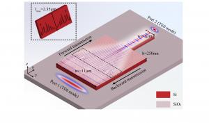
Figure 1 | The working principle of on-chip integrated metalens. Inset: Structure morphology of the optimized on-chip metalens.
Photonic integrated circuits consist of a series of interconnected photonic integrated devices, which have the advantages of low cost, low power consumption, high speed, large bandwidth, and high integration, and are widely used in communications, chip-scale optical signal processing, and biomedical sensing. Since integrated photonic devices, such as grating couplers, wavelength splitters, mode converters, etc., usually have different input/output dimensions, waveguide tapers are required to achieve optical interconnection between different devices. However, when the width scaling ratio of the two connected devices is too large (>10:1), the waveguide taper typically requires hundreds of microns in length to achieve high efficiency and high mode purity transmission of the guided waves. Thus, it limits the further development of on-chip integrated photonic devices toward high integration and hinders the practical application of integrated photonic circuits.
Metalens, as a typical subwavelength photonic device, has been introduced in photonic integration circuits for on-chip optical interconnection in recent years, providing an opportunity to solve the above-mentioned problem of low efficiency of optical interconnection between devices with large scaling.
Nevertheless, the conventional design of the unit cell structure of the metalens is based on periodic boundary conditions which ignore the coupling between the adjacent structures, resulting in errors between the actual and the ideal phase distribution. In particular, when the NA is large (large width scaling ratio), the loss from this error becomes more significant, limiting the device performance at high integration interconnects.
As shown in Figure 1, the research team from the Institute of Optoelectronics Technology of the Chinese Academy of Sciences has proposed a topological optimization-based on-chip metalens design method. The free-form metalens obtained by optimization can realize the highly efficient optical interconnection between waveguide devices with high width scaling ratio, which enables the dual functions of beam focusing and collimation in different waveguide transmission directions.
The relevant results are published in Light: Advanced Manufacturing under the title of “High-fidelity mode scaling via topological-optimized on-chip metalens for compact photonic interconnection”
This work designs parabolic-shaped phase distribution and takes the structure obtained by conventional phase matching method as the initial structure for topology optimization. The transmission efficiency of the TE0 mode at the output port is considered as the optimization target for the optimized design of the silicon waveguide structure shape, which finally realizes the optical interconnection between waveguides of 11 μm and 1 μm in width.
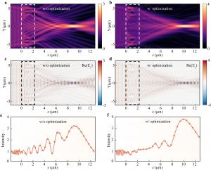
The forward transmission (from wide waveguide to narrow waveguide) achieves efficient focusing for TE0 mode with a relative transmission efficiency of 96%. Figure 2 shows the comparison of the electric field distribution of metalens before and after optimization. The optimized metalens has significantly less stray light when the light enters the narrow waveguide, and a large amount of energy converges at the focal point, resulting in a more desirable focal spot at the desired focal distance, a deeper depth of focus, and a higher focusing efficiency.
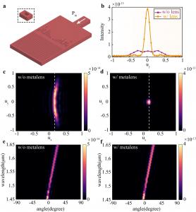
For the collimated mode of backward transmission (from narrow waveguide to wide waveguide), the metalens maintains 69% transmission efficiency for the TE0 mode, which is far higher than that of the traditional waveguide taper (<10%) with the same width scaling. As shown in Figure 3, the designed device ensures the generation of isophase surfaces in the directional radiator, and a resultant higher quality of radiation with less noise as compared with that of the conventional waveguide taper.
This work provides new ideas for optical interconnect design and wavefront shaping in high-integration photonic integrated circuits, and the proposed design approach will find potential applications in the fields of directional radiator, LiDAR, on-chip optical information processing, analog computing, imaging, etc.
###
References
DOI
10.37188/lam.2023.020
Original Source URL
https://doi.org/10.37188/lam.2023.020
Funding information
This research was funded by National key research and development program under Grant 2021YFA1401000; National Natural Science Foundation of China (NSFC) under Grant: 62222513 and U20A20217; Postdoctoral Science Foundation of Sichuan under Grant J22S001.
About Light: Advanced Manufacturing
The Light: Advanced Manufacturing is a new, highly selective, open-access, and free of charge international sister journal of the Nature Journal Light: Science & Applications. It will primarily publish innovative research in all modern areas of preferred light-based manufacturing, including fundamental and applied research as well as industrial innovations.
Wendy Chen
TranSpread
+1 865-405-5638
email us here
Legal Disclaimer:
EIN Presswire provides this news content "as is" without warranty of any kind. We do not accept any responsibility or liability for the accuracy, content, images, videos, licenses, completeness, legality, or reliability of the information contained in this article. If you have any complaints or copyright issues related to this article, kindly contact the author above.


