WIN Semiconductors Releases Next Generation mmWave Enhancement/Depletion GaAs Technology
PQG3-0C platform integrates optimized power and low noise transistors, PN diodes, E/D logic and RF switches on a chip to meet mmWave performance requirements
WIN Semiconductors Corp. (TPEx:TPEx:3105)
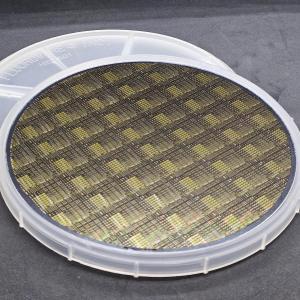
TAOYUAN, TAIWAN, June 13, 2023/EINPresswire.com/ -- WIN Semiconductors Corp (TPEx:3105), the world’s largest pure-play compound semiconductor foundry, announces the commercial release of its next generation integrated mmWave GaAs platform, PQG3-0C. Targeting mmWave front ends, the PQG3-0C technology combines individually optimized E-mode low noise and D-mode power pHEMTs to enable best-in-class PA and LNA performance on the same chip. The E-mode/D-mode pHEMTs have ƒt of 110GHz and 90GHz respectively, and both employ 0.15µm T-shaped gates fabricated by deep ultraviolet stepper technology. Deep UV photolithography is a proven, high volume manufacturing technique for short gate length devices and eliminates the throughput constraints of traditional electron-beam patterning. Offering two application-specific mmWave transistors with RF switches and ESD protection diodes, PQG3-0C supports a wide range of front-end functions with increased on-chip functionality.Both E-mode and D-mode transistors can be used for mmWave amplification and operate at 4V. The D-mode pHEMT targets power amplifiers and provides over 0.6 watt/mm with 11dB linear gain and close to 50% power added efficiency when measured at 29GHz. The E-mode pHEMT operates best as a single supply LNA and delivers minimum noise figure below 0.7dB at 30GHz with 8dB associated gain, and third order output intercept (OIP3) of 26dBm.
The PQG3-0C platform is manufactured on 150mm GaAs substrates and provides two interconnect metal layers with low-k dielectric crossovers, PN-junction diodes for compact ESD protection circuits, and RF switch transistors. With a final chip thickness of 100µm, a backside ground plane with through-wafer-vias (TWV) are standard and can be configured as through-chip RF transitions to eliminate the adverse impact of bond wires at millimeter wave frequencies. PQG3-0C also supports flip-chip packaging and can be delivered with Cu-pillar bumps fabricated in WIN’s internal bumping line.
Contact a WIN Semiconductors regional sales manager for information about sample kits and foundry access.
WIN Semiconductors Corp. at the 2023 International Microwave Symposium, booth # 235
WIN Semiconductors Corp. will be showcasing its compound semiconductor RF and mm-Wave solutions in booth #235 at the 2023 International Microwave Symposium being held at the San Diego Convention Center, June 11th through June 16th.
For more information, visit WIN Semiconductors Corp. at https://www.winfoundry.com/en-US
About WIN Semiconductors Corp.
WIN Semiconductors Corp. is the leading global provider of pure-play GaAs and GaN wafer foundry services for the wireless, infrastructure, and networking markets. WIN provides its foundry partners a diverse portfolio of Hetero-junction Bipolar Transistor and Pseudomorphic High Electron Mobility Transistor, Gallium Nitride High Electron Mobility Transistor, PIN Diode and Optical Device technology solutions that support leading edge products for applications from 50 MHz to 170 GHz and through light-wave. Custom products built by WIN Semiconductors Corp. are found in a vast array of markets, including smartphone, mobile infrastructure, 3-D sensing, optical communications, CATV, aerospace, defense, satellite, and automotive applications.
For over 20 years, WIN has provided foundry services from its state of the art, ISO9001/14001 certified 150mm GaAs facility headquartered in Taoyuan City, Taiwan. This multi-site manufacturing facility has approximately 3000 employees and provides WIN customers with a diverse array of device technology platforms and value-added services, including DC/RF product testing, Cu wafer bumping and advanced package solutions for accelerated product development.
Kara Harmon
WIN Semiconductors Corp.
+1 952-356-5267
kharmon@use.winfoundry.com
Legal Disclaimer:
EIN Presswire provides this news content "as is" without warranty of any kind. We do not accept any responsibility or liability for the accuracy, content, images, videos, licenses, completeness, legality, or reliability of the information contained in this article. If you have any complaints or copyright issues related to this article, kindly contact the author above.

