Nonvolatile and reconfigurable two-terminal electro-optic duplex memristor based on III-nitride semiconductors
USA, August 30, 2024 /EINPresswire.com/ -- An electro-optic duplex memristor on a GaN/AlScN hetero-structure based Schottky diode has been realized. This two-terminal memristor shows good electrical and opto-electrical nonvolatility and reconfigurability. For both electrical and opto-electrical programming modes, the current on/off ratio can reach the magnitude of 104, and the resistance states can be effectively reset, written and long-termly stored.
In the digital age, data storage and processing speed have become key bottlenecks in technological development. Especially with the promotion of artificial intelligence and Internet of Things technology, higher requirements have been put forward for the perception, storage, and processing of massive data. Traditional memory devices have drawbacks such as slow data transmission and high power consumption, and there is an urgent need for a new storage technology to break through this bottleneck.Recently, the research team led by researcher Prof. Li Dabing and Sun Xiaojuan from Changchun Institute of Optics, Fine Mechanics and Physics, Chinese Academy of Sciences, published research results on the journal Light: Science&Applications with the title of "Nonvolatile and reconfigurable two-terminal electro-optic duplex memristor based on III-nitride semiconductors", providing a possible solution to this problem. Their non-volatile optoelectronic duplex memristor based on III-Nitride semiconductors not only performs excellently in electrical storage performance, but also has the characteristic of optically controllable storage, opening up a new path for future intelligent computing and data storage.
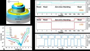
They successfully implemented a Schottky diode type nonvolatile opto-electronic duplex memristor based on AlScN/GaN heterojunction, as shown in Figure 1a. This memristor cleverly combines the excellent ferroelectric properties of AlScN material with the excellent optoelectronic properties of GaN material, enabling it to exhibit excellent performance in both electrical and optical storage modes.
In the electric storage mode, the change in resistance state of the memristor is caused by the ferroelectric polarization inversion of the AlScN layer, which is achieved by affecting the depletion width and electron transfer barrier height of the device. In the study, it was found that by applying bias voltages in different directions, the ferroelectric polarization inversion of the AlScN layer can be triggered, as shown in Figure 1b, thereby cycling between the high resistance state (HRS) and low resistance state (LRS), as shown in Figures 1c~e, achieving programmable storage and reading.
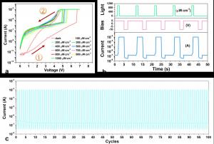
In the photoelectric storage mode, the storage window of the memristor can be controlled by adjusting the light intensity, as shown in Figure 2a. As the light intensity increases, the polarization inversion voltage of the memristor significantly decreases, proving the optical storage performance of the device. This is because the photoconductivity effect in the GaN space charge region and the electron transfer barrier reduction effect caused by photo-generated carriers can adjust the bias applied to the AlScN layer, thereby changing the critical voltage for the overall device resistance state change. Similarly, in the programming mode of “optical write” - “electrical read” - “electrical erase”, the device exhibits good reconfigurable characteristics, as shown in Figures 2b-c.
In addition, they also explored the potential for logical operation applications of the memristor in pure-electrical programming and opto-electronic hybrid programming modes. Through the collaborative work of two memristor devices and external resistors, the "IMP" truth table and logic "False" operation have been successfully reproduced, demonstrating its broad application prospects in the field of memory computing.
DOI
10.1038/s41377-024-01422-4
Original Source URL
https://doi.org/10.1038/s41377-024-01422-4
Funding information
This work is supported by the National Key R&D Program of China [2021YFA0715600]; National Natural Science Foundation of China [62121005, U22A2084]; Youth Innovation Promotion Association of CAS [2023223]; Natural Science Foundation of Jilin Province [20230101345JC, 20230101360JC, SKL202302026]; Young Elite Scientist Sponsorship Program by CAST [YESS20200182].
Lucy Wang
BioDesign Research
email us here
Legal Disclaimer:
EIN Presswire provides this news content "as is" without warranty of any kind. We do not accept any responsibility or liability for the accuracy, content, images, videos, licenses, completeness, legality, or reliability of the information contained in this article. If you have any complaints or copyright issues related to this article, kindly contact the author above.


