Nanusens solves challenges of 6G RF front end design with its RF DTCs
Building on its solutions that unlock upper 5G bands
PAIGNTON, DEVON, UNITED KINGDOM, July 18, 2024 /EINPresswire.com/ -- Nanusens has announced that it has used its pioneering MEMS-within-CMOS™ technology to create a novel solution to the challenge of creating better RF front ends for 6G.Josep Montanyà, Nanusens’ CEO, explained, “This builds on and extends the company’s work of using its unique technology to enable the upper 5G bands to be used cost effectively. We have test chips for this with customers and they are impressed with their performance and actually advised us to use this technology to also create solutions for 6G as the industry really has a challenge.
“The issue is that 6G needs to be able to handle many more and possibly higher frequencies than 5G. To do this requires additional antennas to be integrated into the phone to handle more bands but, due to them having to be smaller to fit more of them inside the phone, their efficiency decreases. In order to get the best possible performance from each antenna, each needs to be tuned to reconfigure to different bands and to avoid mismatch with the power amplifier. This is currently done by means of tunable capacitors.
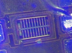
The company has used its patented, silicon-proven technology of building MEMS structures using standard CMOS technologies to create numerous, digitally tunable, nanoscale capacitors within the CMOS layers of a chip along with the control circuitry at the same time. This single chip, integrated solution is smaller than rival solutions and provides much better performance due its much better linearity which means there is virtually zero distortion. In addition, as the nano-capacitors are more power efficient, talk times are up to 30% better and thus solving the current issue of decreased efficiency.
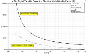
These RF Digitally Tunable Capacitors (DTCs) also solve the issue of current antenna solutions become increasingly power hungry in the higher frequency bands. The key is the very high Q factor of above 100 at 1GHz and, importantly, the Q factor continues to be high up through to the higher bands to keep power losses very low, where the Q factor of rivals drops down significantly. The practical result is an increase in range by around 14% or more which improves user experience as there are fewer dropped calls or poor reception areas.
Dr Marc Llamas, Nanusens’ CTO, said, “Our unique solution for the 5G and 6G RF Front End is exciting the major RF corporations that we have shown it to who need a better solution. We believe that this is RF Front End solution that they have been looking for to enable the 6G market to really take off. Not only for phones but also for other applications in industry and automotive due to its much lower latencies and data rates that are 50 times better than 5G at 1000 gigabits per second. That is a huge potential 6G market that is measured in the hundreds of millions of new devices a year. driven by the rapidly growing needs of data intensive applications such as AI, virtual reality, augmented reality and IoT. Our unique technology of just using standard CMOS techniques in any CMOS fab means that we can produce in virtually unlimited volumes to meet this demand.”
The problem with solid-state switches is that they have a low Q factor, which is a measure of the performance with higher Q factors being better as these indicate lower losses during operation. Solid-state switching solutions’ low Q factor is due to their ON state (Ron) resistance. This becomes worse as the frequency goes up to the higher 5G bands, which has become a limiting factor in using these higher bands effectively. With RF MEMS tunable capacitors, the issue is poor reliability as they use dielectric. This can suffer from dielectric charging which is the main cause of failure in RF MEMS devices and also limits the peak-to-peak voltages that they can withstand before dielectric breakdown.
Nanusens has created a solution that avoids both problems. It uses an array of RF capacitive switches and opens up the implementation of antenna tuning for the higher 6G bands. This solves the low Q factor problem as there is no ON state resistance in this design resulting in a very high Q factor of above 100 at 1GHz and, importantly, the Q factor continues to be high up through to the higher bands to keep losses very low, where the Q factor of rivals drops down significantly. The RF MEMS issues of dielectric charging and/or breakdown do not exist as no dielectric is used in this innovative design. This results in far superior reliability and, as a result, the Nanusens DTCs have successfully passed over four billion switching cycles in the lab without degradation. They are also very robust having been successfully tested for shock, vibration, thermal cycling, MSL 1 and HTSL.
The key factors for DTCs are the Q factor and linearity. The Q factor is above 100 at 1GHz, which matches state-of-the-art RF MEMS solutions and is well above solid-state switching solutions. They also show excellent linearity with more than the 90 dBc for IMD3 which is the 5G requirement.
Minimum capacitance can be kept very small -- down to Coff of 30 fF for a single capacitor off state (that means a Cmin of 0.45 pF for a 4-bit DTC) and even less for future iterations.
Similarly, the capacitance ratio is currently 2.2 and Nanusens expects to improve on this with the next product iteration to 4.
As device performance approaches ideal performance (very low, off-state capacitance (Coff) and very high Q) and new, allocated frequency bands start to move to the microwave domain, parasitics interconnects will increasingly have a negative impact on performance.
Being built using a standard CMOS means that the DTC can be made at the same time and on the same chip as other RF front end components, such as PA, LNA and transceivers, to dramatically reduce interconnect parasitics while making them reconfigurable. These single chip reconfigurable solutions will fit in ultra-small, low profile, low cost WLCSP packages and reduces BOM.
Nigel Robson
Vortex PR
email us here
Visit us on social media:
LinkedIn
Nanusens Digital Tunable Capacitor
Legal Disclaimer:
EIN Presswire provides this news content "as is" without warranty of any kind. We do not accept any responsibility or liability for the accuracy, content, images, videos, licenses, completeness, legality, or reliability of the information contained in this article. If you have any complaints or copyright issues related to this article, kindly contact the author above.


