Researchers develop entangled photon pairs in integrated Silicon Carbide for first time
USA, May 14, 2024 /EINPresswire.com/ -- Quantum science has many fascinating features including entanglement in which pairs of photons1 seem to interact even if physically separated. Integrated quantum photonics (IQP) harnesses such phenomena and enables advancing quantum technology beyond bulky experiments towards real-life uses. Silicon Carbide (SiC) is a promising material for IQP, boasting exceptional characteristics that overcome scalability challenges faced by other materials. Scientists have recently achieved a significant milestone: generating entangled photons from a SiC-based microchip device.
Quantum information science is truly fascinating – pairs of tiny particles can be entangled such that an operation on either one will affect them both even if they are physically separated. A seemingly magical process called teleportation can share information between different far flung quantum systems. These different systems can be coupled using quantum processes to form quantum communication networks. Secure communications, distributed quantum computing and quantum sensing are just some of the remarkable potential applications.
Through more than three decades of Quantum 2.0 – the period of quantum R&D that covers the development of quantum devices, systems and protocols to generate and use quantum entanglement – the vast majority of experiments required bulky optics and specialized alignment schemes often spanning large special purpose optical tables that are pneumatically floating in order to avoid the minutest of mechanical vibrations. In much the same way as miniaturized silicon integrated electronics enabled the evolution of computer processors from large room scale assemblies of capacitors, tubes and magnets to tiny but powerful microchips containing millions and millions of components upon which our modern and ‘smart’ technologies are based; quantum components and processes need to be miniaturized using integrated optics to pave the way for large scale deployment and use of quantum information science beyond lab scale experiments and towards real-life uses.
Silicon carbide (SiC) is a leading platform for integrated processes – powered on in recent years by its use in the integrated electronic systems of green technologies such as electrical vehicles. This application has led to significant improvements in the quality of SiC wafers, the base format for creating integrated devices. In the realm of quantum science, SiC has emerged as a promising material for Integrated Quantum Photonics (IQP), overcoming scalability issues seen in other materials like silicon. SiC's unique properties make it ideal for integrated quantum optical processes, yet challenges persist in harnessing its full potential. Recent breakthroughs in generating entangled photons on SiC microchips mark a significant step toward unlocking its capabilities for practical quantum applications.
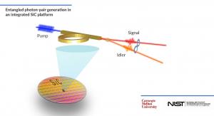
In a new paper (doi: https://doi.org/10.1038/s41377-024-01443-z2) published in Light: Science & Application, scientists at the National Institute of Standards and Technology (NIST) in Gaithersburg, MD and at the Carnegie Mellon University of Pittsburg, PA have reported the first demonstration of a chip-scale entangled photon source in SiC. The device is implemented by a high-order non-linear process known as spontaneous four-wave mixing (SFWM) using an integrated optical microring resonator patterned onto a 4H-SiC-on-insulator platform.
The experiment is designed so that the pairs of photons (signal and idler) are at the telecom wavelength and ideal for being transmitted in optical fibers (which is important for quantum communications and quantum networking) and are created in such a way as to be entangled in time and energy (known as time-energy entanglement). The researchers report generating high-quality and high-purity entangled photon pairs.
These researchers summarize the features of new device, stating "Our results, including a maximum coincidence-to-accidental ratio > 600 for an on-chip photon pair rate of (9 ± 1) × 103 pairs/s and pump power of 0.17 mW, a heralded 𝑔 (2) (0) on the order of 10−3, and a visibility of a two-photon interference fringe exceeding 99% unequivocally demonstrate that integrated SiC-based devices can be viable for chip-scale quantum information processing. In addition, these results are comparable to those obtained from more mature integrated photonic platforms such as silicon."
"We believe that our study lends strong support to the competitiveness of the 4H-SiC-on-insulator platform for quantum applications. For example, the demonstrated entangled photon source can be readily deployed in a fiber-optic network for quantum communication. In addition, by aligning the wavelength of the idler photon to the zero-phonon line of various color centers found in SiC, we can create entanglement between the signal photon and the spin state. This wavelength alignment process can also be integrated and implemented either through chip-scale dispersion engineering or frequency conversion", they added.
The future for SiC-based integrated optics is certainly promising as the researchers offer that "all of these possibilities point to a bright future for SiC-based quantum photonics by enabling the integration of a multitude of chip-scale quantum photonic and electrical processes with color centers for various applications."
DOI
10.1038/s41377-024-01443-z
Original Source URL
https://doi.org/10.1038/s41377-024-01443-z2
Funding information
This work was supported by the Building the Future Program of the Information Technology Laboratory (ITL) at NIST. This work is supported by the NSF (2127499) program at CMU.
Lucy Wang
BioDesign Research
email us here
1 https://doi.org/10.1038/s41377-024-01443-z
2 https://doi.org/10.1038/s41377-024-01443-z

